Imaging the complex streaming patterns of electron flow in graphene field-effect transistors, researchers from RWTH Aachen University and AMO GmbH have found evidence for local spots of viscous electron flow even at room temperature in devices with moderate mobility, implying that viscous electron flow is omnipresent in graphene devices. The results have been reported in Nano Letters.
The strength of graphene for electronic applications roots in its immunity against certain scattering effects. Quantum mechanical interference prohibits the electron backscattering at extended obstacles, leading to a significantly larger electron velocity than in classical semiconductors. The electron mobility in graphene at room temperature can indeed be a factor hundred larger than in silicon. The avoided stopping by obstacles raises the fundamental question what eventually limits the electron mobility. Interestingly, it can be the very same effect as in water flow: viscosity.
Viscosity describes the interaction between particles that transfers the friction at the surrounding walls throughout the streaming fluid. The transmitted friction eventually decelerates the whole fluid. The relevance of viscous effects on the flow of electrons in graphene has indeed been demonstrated, but so far only in very clean samples with low disorder and high mobility. The much more natural situation that both disorder and viscosity jointly suppress the electron velocity has not been studied in experiments.
Researchers from RWTH Aachen University and AMO GmbH tackled this question by imaging the electrostatic potential that results from electron flow. They probed a graphene field-effect transistor fabricated with a scalable technology, using a small metallic tip mounted on a cantilever to detect the potential induced by the current flowing through the device (Fig. 1a). The tip is repelled or attracted by the current-induced potential and it can map the potential strength with a spatial resolution of about 20 nm (Fig. 1b). A complex background subtraction allows to distinguish the potential induced by the current flow from other effects.
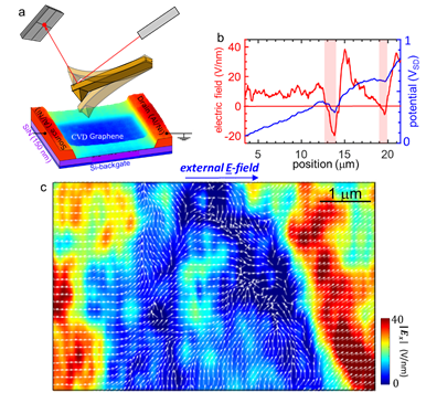
The potential patterns induced by the current in the graphene device – and hence the in-plane electric field patterns – turned out to depend heavily on the electron density of graphene. For a high electron density, the pattern is rather uniform, as in conventional metals, but it gets much more complex at low electron density (Fig. 1c). Here, the electric field within the graphene plane is partly even pointing against the charge flow (highlighted areas in Fig.1b), indicating that electrons move uphill – similar to turbulent water that is flowing against the general direction of flow, e.g., behind an obstacle.
The authors carefully investigated these regions of tentative uphill flow and found that they typically exhibit the lowest disorder density, so that the electrons get faster in these areas, favoring the appearance of viscous effects. They also showed that the effect of uphill stream can be completely suppressed by artificially increasing the defect density by mild bombardment with Argon ions.
The first author of the paper Sayanti Samaddar, now at the National Physics Laboratory in London, summarizes: “Our results indicate that electron viscosity is not an exotic effect present only in ultraclean graphene samples, but that it is present also in “everyday graphene devices” produced with scalable techniques, like those we might find in future commercial applications of graphene.” Zhenxing Wang, leader of the Graphene Electronic Group at AMO GmbH and co-author of the paper adds: “This nice result popped up from a spontaneous cooperation between physicists and engineers, here in Aachen, and might be relevant for us as engineers too, for better understanding the behavior of our devices.”
Bibliographic information:
Evidence for Local Spots of Viscous Electron Flow in Graphene at Moderate Mobility
S. Samaddar, J. Strasdas, K. Janßen, S. Just, T. Johnsen, Z. Wang, B. Uzlu, S. Li, D. Neumaier, M. Liebmann, and M. Morgenstern, Nano Letters 21, 9365 (2021). [arXiv:2103.11466]