Good news for the community working on two-dimensional materials in Europe: a team of researchers at RWTH Aachen University has successfully implemented the process for growing high-quality hexagonal Boron Nitride at atmospheric pressure and high temperature, increasing the resilience of the supply chain of this unique material.
Hexagonal Boron Nitride (hBN) plays a special role in the field of two-dimensional (2D) materials as it is one of the very few 2D insulators available today with very high crystalline quality. Most state-of-the-art electronic devices based on 2D materials include one or more flakes of hBN used as substrate and encapsulation material. And most of this hBN stems from a single source: namely the laboratory of Takashi Taniguchi and Kenji Watanabe at the National Institute of Material Science in Tsukuba, Japan.
Taniguchi and Watanabe are the real pioneers of the field of high-quality hBN and have provided hundreds of labs around the world with high quality hBN crystals. Without their contribution, much of the progress of the last decade in the field of graphene and 2D materials would have literally not been possible. Their growth method, however, is hard to reproduce elsewhere, as it involves both high temperature (more than 1500°C) and extremely high pressure (more than 40.000 times the atmospheric pressure), which are reached with a hydraulic press similar to those used for artificial diamonds.
The group of Taniguchi and Watanabe has also developed an alternative approach to grow hBN in less demanding experimental conditions. The method, which still involves very high temperature (up to 1550°C) but works at atmospheric pressure, has been later substantially optimized by the group of James Edgar at Kansas State University, to the point that it is now on-pair with the original high-pressure approach in terms of quality of the resulting hBN flakes. This advancement has been already reproduced by scientist in China. In Europe there has been, however, no academic supplier of high-quality hBN so far. A team of physicists and chemists at RWTH Aachen University has now closed this gap and successfully implemented the growth process of hBN at room pressure.
“I think this is important news for the community working on 2D materials in Europe, as it ensures the resilience of the supply chain of high-quality hBN, which is a material necessary to many labs,” says the coordinator of the project, Christoph Stampfer from the Physics Department at RWTH Aachen University. “The growth process implemented in Aachen is not really a scientific advancement, but it represents an important achievement form the technological point of view, which we reached thanks to the collaboration with group of Paul Kögerler, from the Institute of Inorganic Chemistry at RWTH, and the support of James Edgard.”
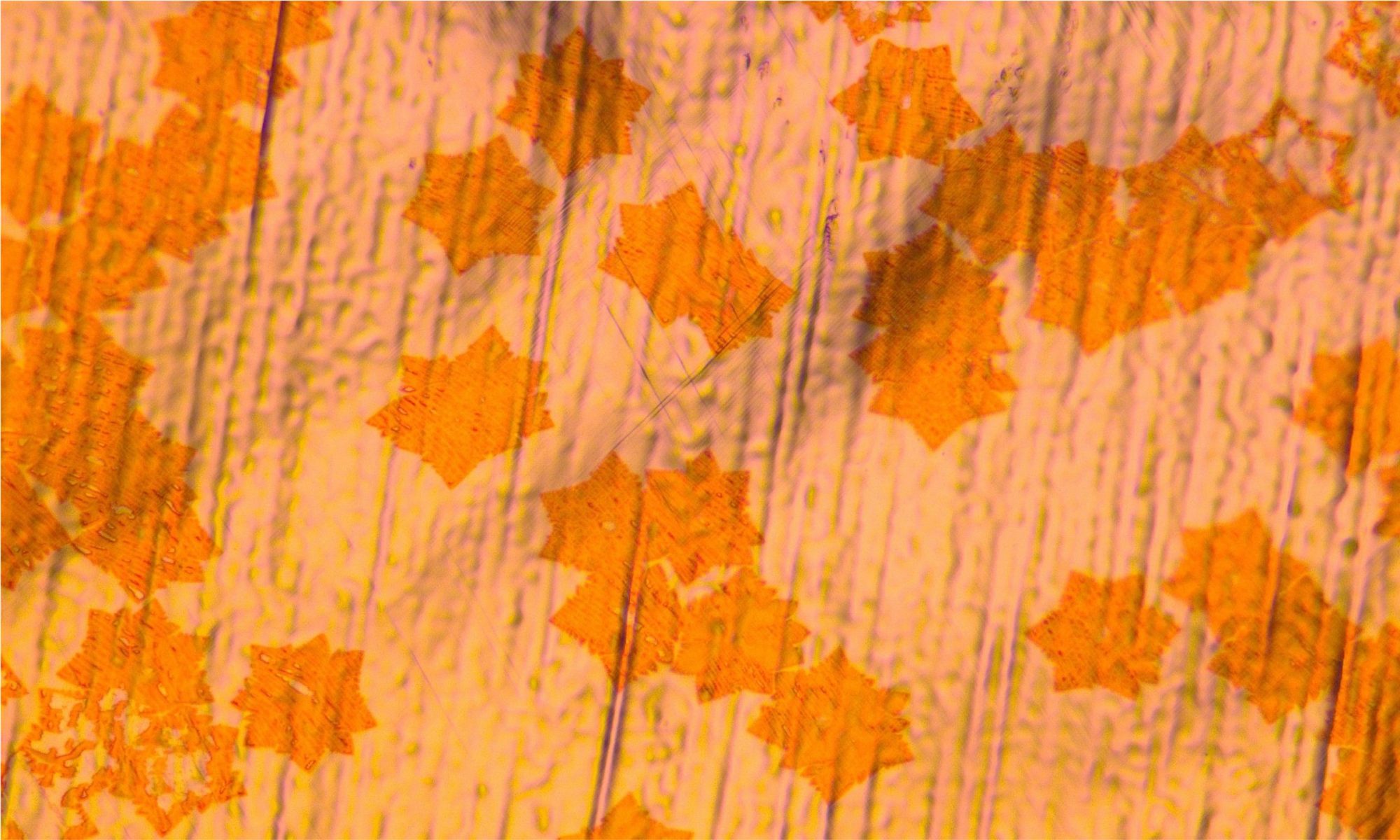
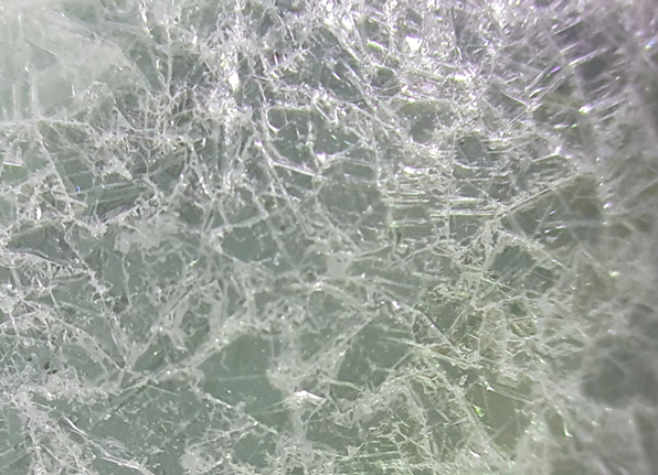
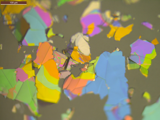
The team around Stampfer and Kögerler has put together the expertise of the two groups to develop a holistic approach to the growth and characterization of the hBN. The growth process implies melting and cooling iron and boron under very controlled conditions and constant nitrogen flow. The result of the process – which takes more almost 7 days – is an iron ingot partially covered by a continuous crystal-layer of hBN. The next critical step is to detach the hBN from the iron. The RWTH team has demonstrated that it is possible to do this in a single step using hydrochloric acid, and that this wet-chemistry step does not affect the quality of the hBN itself. The characterization involved both Raman spectroscopy as well as electrical transport measurements on devices based on graphene encapsulated in hBN. The results have been reported in Nanotechnology.
Bibliographic Information:
“Chemically detaching hBN crystals grown at atmospheric pressure and high temperature for high-performance graphene devices”
T. Ouaj, L. Kramme, M. Metzelaars, J. Li, K. Watanabe, T. Taniguchi, J. H. Edgar, B. Beschoten, P. Kögerler, and C. Stampfer, Nanotechnology, 34 475703 (2023)
DOI: https://doi.org/10.1088/1361-6528/acf2a0
Contact:
Prof. Christoph Stampfer
RWTH Aachen University,
II Institute of Physics
52074 Aachen (Germany)
email: stampfer@physik.rwth-aachen.de