The exceptional electronic properties of graphene make it a material with large potential for low-power, high-frequency electronics. However, the performance of a graphene-based device depends not only on the properties of the graphene itself, but also on the quality of its metal contacts. The lack of effective and manufacturable approaches to establish good ohmic contacts to a graphene sheet is one of the factors that limit today the full application potential of graphene technology.
Continue reading “A scalable method to reduce the contact resistance of graphene”A non-destructive way to probe inter-layer coupling on millimeter-scale graphene-MoS2 heterostructures
One of the great assets of two-dimensional (2D) materials is the possibility of placing different materials on top of each other to form heterostructures with properties tailored to specific application scenarios. However, the quality of the final material stack strongly depends on the electronic coupling between the different materials. Measuring this coupling in a non-destructive way is therefore an important aspect for material development. Researchers from AMO GmbH, RWTH Aachen University and AIXTRON SE have now established a methodology based on Raman spectroscopy for estimating quantitatively the coupling between graphene and molybdenum disulfide (MoS2) in heterostructures up to the mm2-scale.
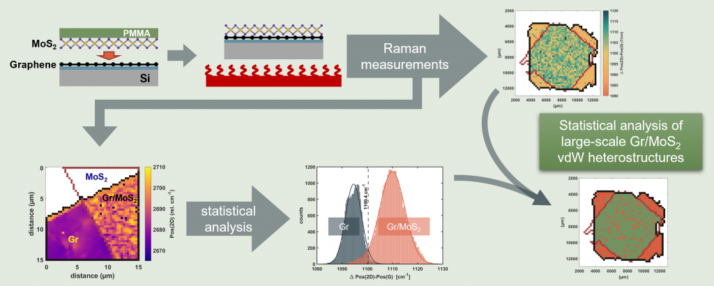
The study focused on 2D materials grown with scalable approaches – specifically graphene grown by chemical vapor deposition and MoS2 grown by metal-organic chemical vapor deposition. The first achievement of the work is the development of a wet-transfer fabrication process for heterostructures spanning mm2-scale areas. The heterostructures were then systematically investigated using Raman spectroscopy. Key findings include:
- Quantitative analysis: The study demonstrates a methodology for discriminating between regions of coupled MoS2/graphene heterostructures and regions where 2D materials are stacked but electronically uncoupled.
- Impact of Annealing: The method was then used to investigate the effects of annealing on the coupling between graphene and MoS2. While annealing supports the formation of closely coupled heterostructures, the study found that varying annealing parameters did not significantly impact the results.
- Scalability and Variability: By extending the analysis to larger scale heterostructures, the research highlights the variability in coupling strength across different areas, emphasizing the need for further optimization in assembly techniques.
- Raman-Based Methodology: The proposed non-destructive Raman spectroscopy approach emerges as a promising tool for industrial implementation, enabling the evaluation of electronic coupling in 2D material heterostructures on a large scale.
For more information and to access the full study, please visit https://doi.org/10.1016/j.mne.2024.100256.
Bibliographic information
N. Rademacher, E. Reato, L. Völkel, A. Grundmann, M. Heuken, H. Kalisch, A. Vescan, A. Daus, M. C. Lemme,
CVD graphene-MoS2 Van der Waals heterostructures on the millimeter-scale,
Micro and Nano Engineering (2024)
https://doi.org/10.1016/j.mne.2024.100256.
First demonstration of a CMOS inverter based on transition metal dichalcogenides on a flexible substrate
Researchers of the Aachen Graphene and 2D Materials Center have demonstrated the first CMOS inverter based on transition metal dichalcogenides (TMDC) on a flexible substrate, using two distinct TMDC materials, MoS2 and WSe2.
Continue reading “First demonstration of a CMOS inverter based on transition metal dichalcogenides on a flexible substrate”An effective method to measure the adhesion of 2D materials
One of the big selling points of two-dimensional (2D) materials is their self-passivated nature, which allows them to be deposited on any substrate and opens up new possibilities for three-dimensional material stacks. The downside is their weak adhesion to the substrate, which can be a source of device instability. Quantifying the adhesion of 2D materials to three-dimensional surfaces is therefore an essential step for the reliable integration of devices based on 2D materials. A team of researchers around Max Lemme has now shown that the adhesion between 2D materials and substrates can be efficiently quantified using button-shear testing.
Continue reading “An effective method to measure the adhesion of 2D materials”An automatic flake-search tool for 2D materials
Researchers at the Aachen Graphene & 2D Materials Center have released an open-source platform to automatically identify and classify exfoliated flakes of two-dimensional (2D) materials on a substrate, shortening one of the most time-consuming and tedious tasks in the study of 2D materials.
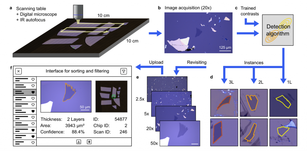
In their 2013 perspective article on van der Waals heterostructures, Geim and Gregorieva introduced the effective analogy of 2D materials as atomic-sized Lego blocks. The analogy illustrates well not only the sheer variety of structures that can be realized by stacking different 2D materials, but also a common bottleneck in the fabrication process: finding the right piece. As any avid Lego builder knows, finding a piece of the right size and shape can take time and patience. The same is true in the 2D materials community, where researchers often spend hours at the microscope, manually scanning exfoliated 2D-material flakes to find a crystal with the desired properties. The team of Prof. Christoph Stampfer at RWTH Aachen University has now developed an efficient tool to automatically detect and classify 2D material flakes and has made the source code openly available.
“Our goal was to develop a truly competitive alternative to the manual search by a patient and well-trained researcher,” says Jan-Lucas Uslu, who has been the main driving force behind the project. The fully automated workflow developed by Uslu and his colleagues starts at the very end of the exfoliation process, when the flakes are deposited on a silicon oxide substrate. Using classical machine learning models and a microscope with motorized scanning stage and motorized objective revolver, the system is able to reliably detect and classify all the flakes present on a substrate, indicating the number of layers of each flake, as well as its shape and dimensions. All of this information is then conveniently stored in an interactive database, along with images of the flakes taken at various resolutions. A Demo of the interactive database can be accessed here.
The automated flake search system has been tested in Stampfer’s lab for more than two years. “The effort to develop such a tool has already paid off,” says Stampfer. “Not only have we become much more efficient in assembling heterostructures, but there are also studies that we probably would have never started without a fast and efficient way to find flakes of the desired thickness.” One example is the systematic study of the dielectric screening in WS2-graphene heterostructures as a function of the thickness of the spacer layer, which was varied from one to 16 atomic layers of hBN – a daunting task without the flake-search tool.
The implementation of the automated flake search tool and the associated workflow have now been reported in the IOP journal Machine Learning: Science and Technology, while the source code has been made publicly available via GitHub in a package that includes both the control software and the detection algorithm and training routines, which can also be used as stand-alone software to identify flakes on manually captured images.
In addition to the speed and reliability, one of the attractive features of the detection algorithm is that it can be trained on just a few images, allowing new materials to be quickly integrated into the workflow. “Since the detection is based on the color contrast of the materials, which is a physical property, the training could in principle be replaced by simulations.” says Uslu.
Bibliographic Information:
An open-source robust machine learning platform for real-time detection and classification of 2D material flakes
J.-L. Uslu, T. Ouaj, D. Tebbe, A. Nekrasov, J.H. Bertram, M. Schütte, K. Watanabe, T. Taniguchi, B. Beschoten, L. Waldecker, and C. Stampfer, Mach. Learn.: Sci. Technol. accepted (2024) (or: arXiv: 2306.14845)
A workshop in Aachen on “2D Materials for Future Electronics”
AMO GmbH and the Aachen Graphene & 2D Materials Center are organizing a two-day workshop on “2D Materials for Future Electronics”, in cooperation with RWTH Aachen University and the University of Wuppertal.
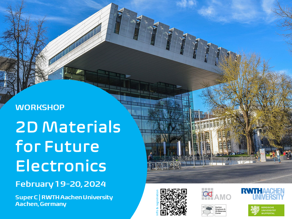
The workshop will take place on February 19-20, 2024 in the scenic lecture halls of the SuperC building, in Aachen. The scope of the workshop is to discuss the opportunities offered by 2D materials for future electronics, as well as the challenges that still need to be solved to turn the scientific advancements of the field into marketable innovations.
The program will cover several facets of the field, including:
- massive scaling and miniaturization (“2D materials for more Moore”)
- flexible electronics and sensors (“2D materials for more than Moore”)
- novel computing paradigms (“2D materials for neuromorphic computing”).
The workshop will also feature a special hybrid session dedicated to electronics based on transition metal dichalcogenide (TMDs) in cooperation with the 2D-Experimental Pilot Line.
Confirmed speakers:
- Gianluca Fiori (Uni Pisa)
- Michael Heuken (AIXTRON)
- Andras Kis (EPFL)
- Theresia Knobloch (TU Wien)
- Karl Magnus Persson (VTT)
- Dmitry Polyushkin (TU Wien)
- Frank Schwierz (TU Illmenau)
- Quentin Smets (imec)
- Roman Sordan (Politecnico di Milano)
- … more to come!
Original contributions by the participants in form of a poster are warmly welcome.
Participation to the workshop is free, but registration is mandatory due to the limited number of places available. The deadline for registration is February 10, 2024.
More information & registration
The workshop is organized with the financial support of the European Commission, through the projects ORIGENAL, MISEL, 2D-EPL, a nd AttoSwitch, and of the German Federal Ministry for Education and Research (BMBF) through the projects NeuroSys und NEUROTEC.

Scientific organizers: Max Lemme (AMO GmbH & RWTH Aachen University), Daniel Neumaier (University of Wuppertal & AMO GmbH), Zhenxing Wang (AMO GmbH) , Gordon Rinke (AMO GmbH)

First observation of coherent charge dynamics in graphene quantum dots
In a recent study published in Nature Communications, researchers from RWTH Aachen University and Forschungszentrum Jülich have reported the observation of coherent charge oscillations in bilayer graphene quantum dots. This marks a significant milestone on the way to spin and valley qubits in a two-dimensional material system.
High quality hexagonal Boron Nitride – made in Aachen
Good news for the community working on two-dimensional materials in Europe: a team of researchers at RWTH Aachen University has successfully implemented the process for growing high-quality hexagonal Boron Nitride at atmospheric pressure and high temperature, increasing the resilience of the supply chain of this unique material.
Congratulations to Prof. Annika Kurzmann
Prof. Annika Kurzmann has been appointed ML4Q Professor for Experimental Solid-State Physics at the University of Cologne.
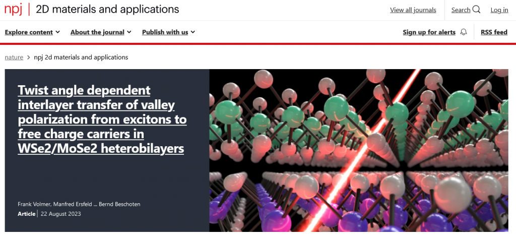
Continue reading “Congratulations to Prof. Annika Kurzmann”Interlayer transfer of valley polarization from excitons to free charge carriers in WSe2/MoSe2 heterobilayers
Scientists from RWTH Aachen, AMO GmbH, Forschungszentrum Julich and the University of Regensburg have shown that in twisted heterobilayers of WSe2 and MoSe2 there is a transfer of valley polarization from excitons in WSe2 to free carriers in MoSe2. This mechanism, which is strongly dependent on the twist angle, may allow the realization of opto-valleytronic devices where the valley polarization is optically excited but extracted and measured by electrical means. The results are reported in npj 2D Materials and Applications.