One of the great assets of two-dimensional (2D) materials is the possibility of placing different materials on top of each other to form heterostructures with properties tailored to specific application scenarios. However, the quality of the final material stack strongly depends on the electronic coupling between the different materials. Measuring this coupling in a non-destructive way is therefore an important aspect for material development. Researchers from AMO GmbH, RWTH Aachen University and AIXTRON SE have now established a methodology based on Raman spectroscopy for estimating quantitatively the coupling between graphene and molybdenum disulfide (MoS2) in heterostructures up to the mm2-scale.
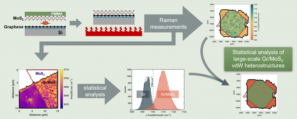
The study focused on 2D materials grown with scalable approaches – specifically graphene grown by chemical vapor deposition and MoS2 grown by metal-organic chemical vapor deposition. The first achievement of the work is the development of a wet-transfer fabrication process for heterostructures spanning mm2-scale areas. The heterostructures were then systematically investigated using Raman spectroscopy. Key findings include:
- Quantitative analysis: The study demonstrates a methodology for discriminating between regions of coupled MoS2/graphene heterostructures and regions where 2D materials are stacked but electronically uncoupled.
- Impact of Annealing: The method was then used to investigate the effects of annealing on the coupling between graphene and MoS2. While annealing supports the formation of closely coupled heterostructures, the study found that varying annealing parameters did not significantly impact the results.
- Scalability and Variability: By extending the analysis to larger scale heterostructures, the research highlights the variability in coupling strength across different areas, emphasizing the need for further optimization in assembly techniques.
- Raman-Based Methodology: The proposed non-destructive Raman spectroscopy approach emerges as a promising tool for industrial implementation, enabling the evaluation of electronic coupling in 2D material heterostructures on a large scale.
For more information and to access the full study, please visit https://doi.org/10.1016/j.mne.2024.100256.
Bibliographic information
N. Rademacher, E. Reato, L. Völkel, A. Grundmann, M. Heuken, H. Kalisch, A. Vescan, A. Daus, M. C. Lemme,
CVD graphene-MoS2 Van der Waals heterostructures on the millimeter-scale,
Micro and Nano Engineering (2024)
https://doi.org/10.1016/j.mne.2024.100256.