We are pleased to announce the DGKK Seminar on Growth Kinetics and Layer Transfer of Ultra-Thin Layers and 2D Materials, taking place November 23–24, 2026, at RWTH Aachen University.
New insights & plenty of discussions!
On 03–04 March 2026, 127 researchers and industry experts gathered at the SuperC at RWTH Aachen University for the 2nd workshop “2D Materials for Future Electronics.” The event proved to be a great success, bringing together a vibrant community to exchange ideas and explore emerging developments in the field.

2nd Workshop on “2D Materials for Future Electronics”
The 2nd Workshop on “2D Materials for Future Electronics” will take place on March 3–4, 2026, in Aachen, Germany, bringing together leading researchers and industry experts for a two-day, in-person exchange on recent advances and future perspectives of two-dimensional materials in electronic applications.
Continue reading “2nd Workshop on “2D Materials for Future Electronics””There’s Plenty of Room at the Top!
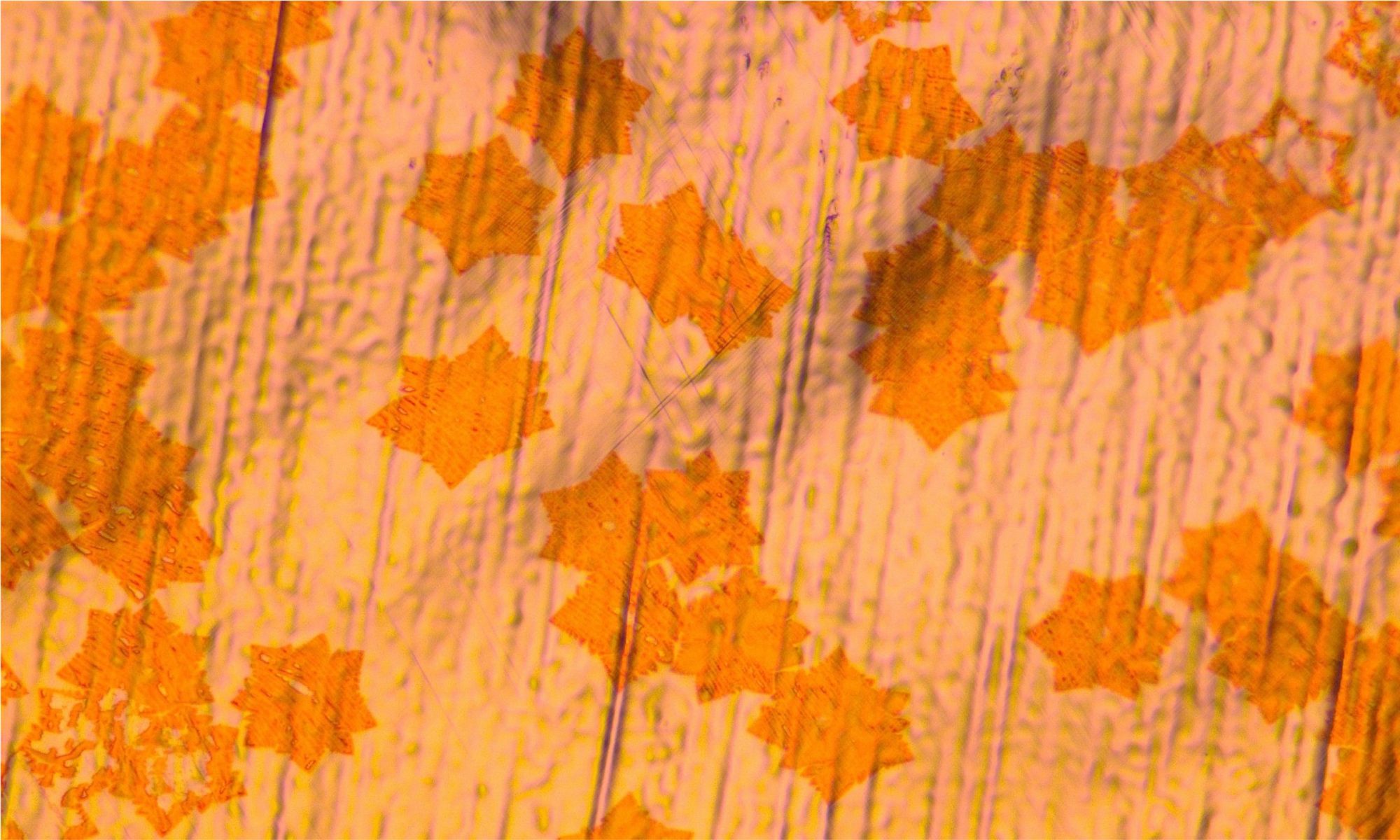
In his famous 1959 lecture “There’s Plenty of Room at the Bottom,” physicist Richard Feynman explored the vast, untapped potential of manipulating matter at the nanoscale. Fast forward to today, and researchers are turning their gaze upward — not downward — to explore a new frontier in electronics.
Continue reading “There’s Plenty of Room at the Top!”Exploring Quantum Geometry with Terahertz Light: A Breakthrough in Twisted Bilayer Graphene
A recent groundbreaking study led by ICFO researchers, in collaboration with several international research groups including memebrs of the Aachen Graphene & 2D Materials Center, has uncovered previously unseen behaviors in magic-angle twisted bilayer graphene using terahertz light. As part of this international effort, the research sheds new light on the quantum geometry of this enigmatic material, revealing how the electronic wavefunctions of electrons are shaped by their environment.
Continue reading “Exploring Quantum Geometry with Terahertz Light: A Breakthrough in Twisted Bilayer Graphene”A succesful event!
The two-day workshop on Novel (2D) Materials and their Applications has been a very succesful event, with 120 participants in presence and plenty of opportunities of discussion and networking. A big thank-you to all participants an, in particular, to all speakers who contributed absolutely excellent talks.
Continue reading “A succesful event!”Forming-free, volatile resistive switching in multilayer MoS₂
Sofia Cruces and co-workers at the Chair of Electronic Devices have recently published an article in Small Science, reporting on forming-free, volatile resistive switching in multilayer MoS₂ grown by metal-organic chemical vapor deposition (MOCVD).
Continue reading “Forming-free, volatile resistive switching in multilayer MoS₂”Workshop announcement: Two exciting days dedicated to “Novel (2D) Materials and their Applications”
The Aachen Graphene & 2D Materials Center is co-organizing an exciting 2-day workshop dedicated to Novel (2D) Materials and their Applications on February 17-18, 2025.
Continue reading “Workshop announcement: Two exciting days dedicated to “Novel (2D) Materials and their Applications””Prof. Maria Fyta has joined the Aachen Graphene and 2D Materials Center
We are thrilled to announce that Prof. Maria Fyta has joined the Aachen Graphene and 2D Materials Center, significantly enhancing the Center’s research profile in computational modeling and the application of 2D materials in biotechnology.
Continue reading “Prof. Maria Fyta has joined the Aachen Graphene and 2D Materials Center”Researching MoS2-based MOSFETS – together with Ukraine
The Chair for Electronic Devices (ELD) at RWTH Aachen University is going to embark on a joint research project with the group of Prof. Alexei N. Nazarov at the Lashkaryov Institute of Semiconductor Physics (ISP) in Kyiv.
Continue reading “Researching MoS2-based MOSFETS – together with Ukraine”