Graphene and related materials are ideal for optoelectronic components in integrated photonic devices, to be used in the next generation of communications systems. Chip-integrated electro-optic devices can significantly increase the performance of datalinks in terms of capacity, lower energy consumption and costs.
Graphene-based integrated photonic devices are promising for faster and low-power data communications. This will be pivotal to meet the further demands on the internet, including 5G and the Internet of Things.
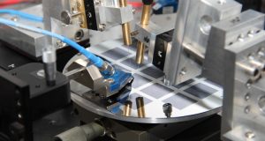
Graphene Flagship researchers based at AMO in Aachen, Germany have demonstrated ultrafast graphene photodetectors with a record bandwidth greater than 76 GHz, suitable for communication links faster than 100 GBits/channel. Published in the Journal of Physics D, these devices are the first graphene photodetectors to be fully fabricated on 6-inch silicon wafers in a semiconductor pilot line, demonstrating scalable fabrication of high-performance graphene based components.
Unlike narrowband compound semiconductors such GaAs, InP, InSb, GaN which are difficult to integrate with silicon, graphene photodetectors are an ideal match to the silicon photonic waveguides, as they offer light detection at different wavelengths, the highest operation speed and a heterogeneous fabrication technology that avoids more expensive techniques, such as molecular beam epitaxy: this all together is so far not offered by other technologies.
Graphene Flagship researcher Daniel Schall and co-workers at AMO employed all the tools of the chip fabrication industry but used a wafer-based process compatible with graphene, taking the next steps towards scalable fabrication of photonic graphene devices. Moreover, the achieved bandwidth record it is a significant step forward towards the goal of chip-integrated high speed optical interconnects.
“Our group has been working for almost one year on fabricating this photodetector,” said the paper’s lead author Daniel Schall. “Considering that process constraints are given, and so it is the available technology, we have successfully overcome the challenge of making a device with high bandwidth. Once we improve its sensitivity, we will get to a point where mass production of these devices becomes truly possible.”
“The Graphene Flagship Work Package Optoelectronics and Photonics aims to develop ultra-fast photodetectors and modulators for data communications applications,” explained Frank Koppens, work package leader, from ICFO, Spain. “This work represents an important step forward in the realisation of these goals. It shows that it is possible to make a very large number of photodetectors on an integrated platform, with a low-cost process and that is exactly what industry wants to see. Moreover, having industrial partners to decide joint research’s goals, it is a huge benefit that accelerates the progress,” he pointed out.
Daniel Neumaier, of AMO, was involved in the research and is leader of the Graphene Flagship’s Electronics and Photonics Integration Division and Electronic Devices Work Package. Speaking about the next steps for this work, he said “Now we need to work on the key parameters for going from a lab demonstration to the final product, increasing reliability, long term stability and fabrication yield. This requires dedicated engineering efforts in close collaboration with the semiconductor foundries involved in the Flagship.”
Taking graphene-based technologies to real-world applications is at the core of the Flagship. “The Graphene Flagship offers a unique environment for collaboration, covering the whole value chain and also all relevant disciplines. This is essential for developing new device concepts and bringing them closer to application, as it requires on one hand input from fundamental physics and material science, but also the knowledge and know-how from different companies, especially those producing the devices and those implementing the device into their systems,” added Neumaier.
The photodetectors presented in this work target applications in optical data communication and microwave photonics by demonstrating the large volume fabrication. This will pave the road to simultaneously integrate these devices also in end-user-devices and increase the speed of data transmission for everyone.
Andrea Ferrari from the University of Cambridge, Science and Technology Officer of the Graphene Flagship and Chair of its Management Panel, stated “With Core 1 the Flagship embarked in the ambitious journey to integrated graphene and related materials with CMOS technology. This is an essential step to bring to fruition the huge opportunities that these materials offer for photonics and optoelectronics. This paper represents yet another key milestone to achieve the final goals of the Flagship, and demonstrates that graphene can be integrated with standard industrial processes.”
Graphene news: https://graphene-flagship.eu/high-bandwidth-graphene-photodetectors-for-high-speed-optical-communications