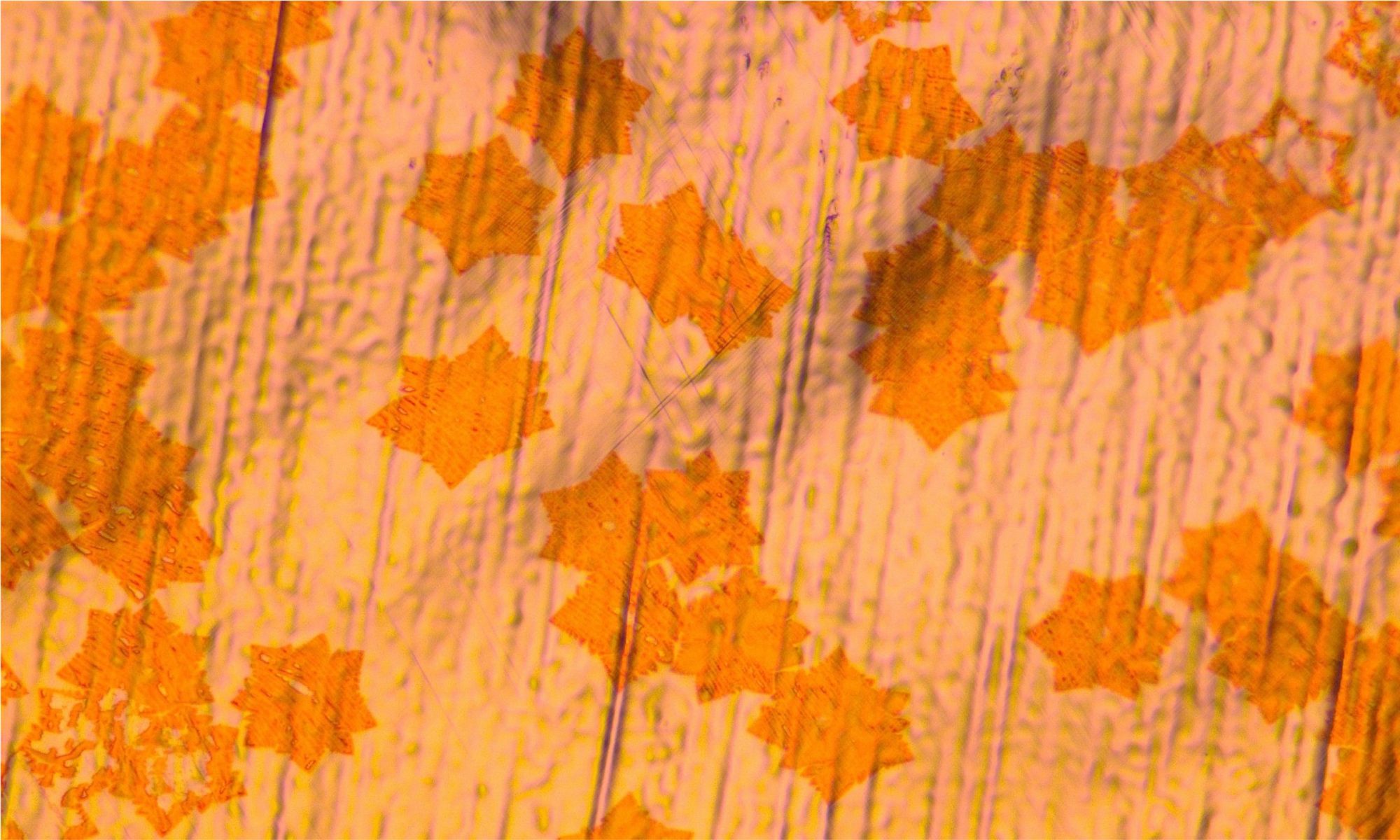
Researchers from RWTH Aachen University, AMO GmbH, Stanford University and IHP have demonstrated that heterostructures formed by silicon, molybdenum disulfide (MoS2) and graphene are potential candidates as emitter-diodes of graphene-base hot-electron transistors.

The concept of hot electron transistors (HETs) was developed already in 1961 by C. Mead at Caltech. HETs are three terminal devices comprised of two back-to-back connected diodes formed by an emitter (n+-Si), a base (typically a metal) and a collector (metal), separated by thin barrier-layers. The first diode is the emitter that injects hot electrons, while the second one is called the filtering diode, as it enables only high-energy electrons to reach the collector.
A main limitation to the performance of HETs is the long electron transit-time in the metallic base. This problem can be circumvented exploiting the unique conduction properties graphene and replacing the metallic base with this material. Simulations show however that high on-state collector currents can be achieved only if the conduction-band offset between the emitter and the injection barrier is small enough for thermionic emission of electrons.
This is where the work of Belete and colleagues becomes interesting from the application point of view. In fact, the observed low barrier between Si and MoS2 and the resulting thermionic emission of hot electrons across Si/MoS2/Graphene vertical heterostructures satisfy the conditions for high on-state currents, and make their devices potential candidates as emitter diodes of graphene-base HETs for future high-speed electronics.
This work has been published on ACS Applied Materials & Interfaces and it is accessible via the following link https://pubs.acs.org/articlesonrequest/AOR-zm63xFhfBR5K2a8Dzj8x. In the next 12 months, the first 50 e-prints will be free of charge for the reader.
The research work was funded by the European Commission (Graphene Flagship, 785219, QUEFORMAL, 829035) the German Ministry of Education and Research, BMBF (GIMMIK,03XP0210, NeuroTec, 16ES1134), and the German Research Foundation, DFG (MOSTFLEX, 407080863).
Bibliographic information:
Electron Transport across Vertical Silicon/MoS2/Graphene Heterostructures: Towards Efficient Emitter Diodes for Graphene Base Hot Electron Transistors
M. Belete, O. Engström, S. Vaziri, G. Lippert, M. Lukosius, S. Kataria and M. C. Lemme
ACS Appl. Mater. Interfaces (2020)
https://pubs.acs.org/doi/full/10.1021/acsami.9b21691
