With what could be a step forward towards large-scale high-performance graphene electronics, a team of German and French scientists has demonstrated the excellent quality of monoisotopic hexagonal boron nitride grown at atmospheric pressure by the group of James Edgar at Kansas State University.
Hexagonal boron nitride (hBN) is the unsung hero of graphene research. Indeed, much of the progress of the last ten years has been enabled by the discovery that sandwiching graphene between two hBN crystals can improve enormously the quality of graphene devices. This has opened the door to a series of exciting developments, including the discoveries of exotic effects such as magic-angle superconductivity and proof-of-concept demonstrations of sensors with unrivalled sensitivity.
Up to now, the best and by far most widely used hBN crystals come from the laboratory of Takashi Taniguchi and Kenji Watanabe at the National Institute of Material Science in Tsukuba, Japan. These crystals are grown using a process based on high temperature (more than 1500°C) and extremely high pressure (more than 40.000 times the atmospheric pressure). “The contribution of Taniguchi and Watanabe to graphene research is invaluable”, says Christoph Stampfer from RWTH Aachen University. “They provide hundreds of labs around the world with ultra-pure hBN at no charge. Without their contribution, a lot of what we are doing today would not be possible.”
The main limitations of the hBN grown by Taniguchi and Watanabe are the crystal size, which is limited to a few 100 µm, and the complexity of the growth process. If this is good for fundamental research, it is a no-go in terms of scalability. “I’ve been very excited when James Edgar proposed us to test the quality of his hBN”, says Stampfer, “as his growth method is in principle suitable for large-scale production”. Edgar’s method for growing hBN at atmospheric pressure is indeed much simpler and cheaper than the one of the Japanese team. Furthermore, it also allows controlling the isotopic concentration.
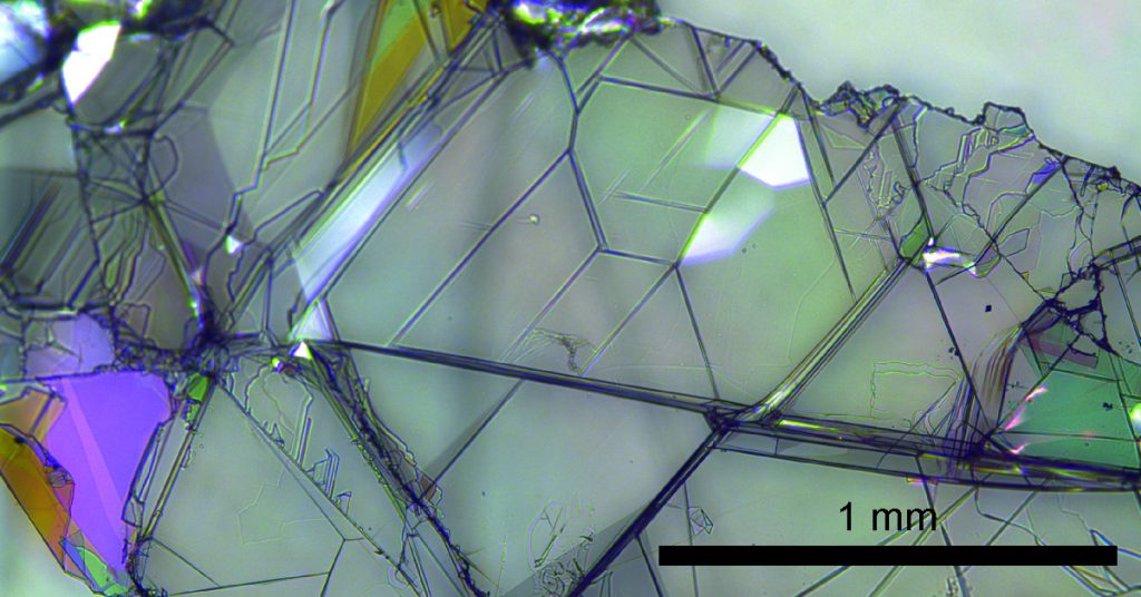
“The hBN crystals we received from Edgar’s group were the largest I’ve ever seen”, says Jens Sonntag, a PhD student in Stampfer’s group, “and they were all based either on isotopically pure 10B or 11B”. Sonntag tested the quality of the flakes first via confocal Raman spectroscopy and then, in a collaboration with the group of Annick Loiseau at ONERA-CNRS, via luminescence measurements. Both types of measurements indicated high isotope-purity and high crystal-quality. However, the strongest evidence of the high quality of Edgar’s hBN came from the transport measurements performed on devices based on graphene sandwiched between monoisotopic hBN. In this type of experiment, the graphene sheet acts as a sensitive detector for disorder in the hBN. The performance of the devices based on monoisotopic hBN turned out to be absolutely equivalent to the one of state-of-the-art devices based on hBN produced by Taniguchi and Watanabe, if not slightly better.
“This is a clear indication of the very high quality of the hBN crystals we received from Edgar’s group”, says Stampfer. “This is great news for the whole graphene community, because it shows that it is in principle possible to produce high-quality hBN on large scale, bringing us one step closer to real applications based on high-performance graphene electronics. And furthermore, the possibility of controlling the isotopic concentration of the crystals opens the door to experiments that were not possible before.” This research has been published open-access on 2D Materials.
Bibliographic info:
Excellent electronic transport in heterostructures of graphene and monoisotopic boron-nitride grown at atmospheric pressure
J. Sonntag, J. Li, A. Plaud, A. Loiseau, J. Barjon, J. H. Edgar, C. Stampfer,
2D Materials (2020, advanced on-line publication)
DOI: https://doi.org/10.1088/2053-1583/ab89e5
Contact:
Jens Sonntag
RWTH Aachen University,
II Institute of Physics
52074 Aachen (Germany)
email: sonntag@physik.rwth-aachen.de