Researchers from AMO GmbH, Oxford Instruments, Cambridge University, RWTH Aachen University and the University of Wuppertal have demonstrated a new method to use PEALD on graphene without introducing defects into the graphene itself.
One thing that has become clear in the last decade of graphene research is that it is necessary to protect the surface of graphene from external contaminants, to preserve its exceptional electronic properties and be able to exploit them into novel devices. The depositions of dielectric materials on top of graphene is therefore an essential step of manufacturing graphene-based electronic and photonic devices.
Presently, the most advanced technique for depositing dielectrics on graphene is atomic layer deposition (ALD), which allows to precisely control the uniformity, the composition and the thickness of the film. The process typically used on graphene and other 2D materials is thermal water-based ALD, as it does not damage the graphene sheet. However, the lack of nucleation sites on graphene limits the quality of the dielectric film, and requires the deposition of a seed layer prior to ALD to achieve good results. Another approach is plasma enhanced atomic layer deposition (PEALD), which, when applied to growth on graphene, can introduce surface damage.
Now, researchers from AMO GmbH, Oxford Instruments, Cambridge University, RWTH Aachen University and the University of Wuppertal have demonstrated a new method to use PEALD on graphene without introducing defects into the graphene itself. The trick is to use one monolayer of hexagonal boron nitride (hBN) – a two-dimensional insulator – as a protection layer on top of graphene. The monolayer hBN is thin enough to have a negligible effect on the quality of the dielectric, but thick enough to protect the graphene from the oxygen plasma used in PEALD Furthermore, the plasma creates nucleation sites on the hBN, which allow the fast growth of high-quality dielectric films.
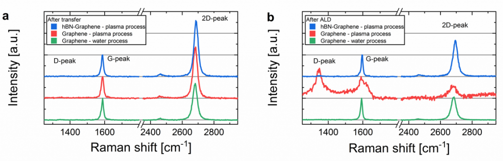
The protective effect of the hBN monolayer is clearly revealed by Raman spectroscopy measurements performed before and after the deposition of the dielectric (see Fig. 1). “The Raman study is very important for the characterization of the graphene and for the optimization of the process”, says Dr. Bárbara Canto, first author of the study. “This can lead us to future graphene devices with higher quality dielectrics and an improved understanding of the effect of the different process steps on graphene”. Electrical characterization of field-effect devices fabricated on the hBN/graphene confirms that the graphene remains undamaged, and demonstrates the high quality of the dielectric.
Ravi Sundaram, Head of Strategic R&D Markets at Oxford Instruments UK, says “This work makes great progress on one of the key challenges in graphene (opto)electronic device manufacturing i.e, the deposition of high quality dielectrics. We are very pleased to have contributed to this multi-organization collaboration, to push the limits of low damage plasma enhanced ALD of dielectrics to enable the integration of these devices in practical applications”.
The results have been published in the last issue of Advanced Materials Technologies.
Bibliographic information:
Plasma-enhanced atomic layer deposition of Al2O3 on graphene using monolayer hBN as interfacial layer
Bárbara Canto, Martin Otto, Michael J. Powell, Vitaliy Babenko, Aileen O’Mahony, Harm C. M. Knoops, Ravi S. Sundaram, Stephan Hofmann, Max C. Lemme, Daniel Neumaier
Advanced Materials Technologies, 2100489 (1-8), 2021.
DOI: https://doi.org/10.1002/admt.202100489
Tags: graphene, PEALD, ULISSES, ORIGENAL, 2D-EPL; ECOMAT, GIMMIK, Graphene Flagship