Dr. Jens Martin, from the Leibniz-Insitut für Kristallforschung (IKZ) in Berlin, has been the speaker of the 30th Aachen Graphene Center Seminar. Dr. Martin is the head of the section Semiconductor Nanostructures at IKZ, and one of the coordinators of the IKZ-IRIS Joint Lab “Layer Transfer for 2D-Heterostructures“. In his talk, presented the recent advances of his group on the growth, release and transfer of thin epitaxial perovskite films, as well in on the in-situ growth of 2D-vdW multilayers and heterostructures.
TITLE: New perspectives on Layer Transfer and Artificial Crystalline Heterostructures
ABSTRACT: Layer transfer introduces a paradigm shift in the way crystalline heterostructures could be synthesized. In contrast to established growth methods of epitaxial heterostructures which must oblige to matching conditions at the interface with respect to surface energies, lattice parameter and crystal symmetry, layer transfer allows in principle for the combination of any crystalline materials.
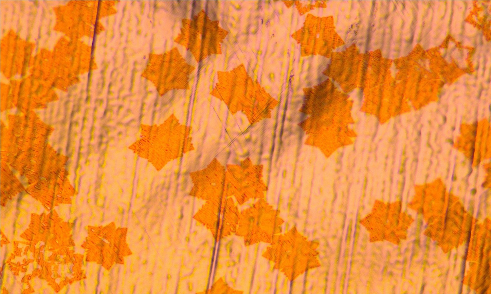
In particular, the potential to create novel artificial crystalline heterostructures has been demonstrated with 2-dimensional van der Waals (2D-vdW) materials. New functional interfaces can be realized by novel combinations of different 2D-vdW-materials. More astonishing, emerging physical properties can be produced by re-assembling layers of the same material in different ways, for example by introducing a twist angle between the layers. In this way so-called Moiré-materials can be created which for 2D-vdW materials allow for unique ways of band structure engineering, famously the formation of flat bands at magic angle twisted bilayer graphene. It also has been realized that stacking of 2D-materials creates periodic strain patterns. Yet, because the interlayer interaction in 2D-vdW materials is intrinsically weak and intralayer bonds are always stronger, it is not possible to create defect structures within the layer, that is to produce artificial twist boundaries characterized by screw-dislocation networks. This is different with covalently or ionic bonded materials such as oxides. For example, in oxidic perovskites the bonding character is almost ionic, making it possible to produce nm-thin films in (100)-orientation virtually without surface reconstruction. Yet interaction to other polar surfaces remains strong, and as demonstrated in the past via wafer bonding of single crystals, dislocation networks at the interface occur after thermal annealing.
The potential of layer transfer for future crystal assembly has been recognized by Leibniz-Institut für Kristallzüchtung (IKZ). After providing a brief general overview of the IKZ, and the research activities of the section “Semiconductor Nanostructures”, I will discuss preliminary results on growth, release and transfer of thin epitaxial perovskite films. As outlook, we propose that artificial twist boundaries in nm-thin perovskite films can serve as innovative nano-engineering platform for epitaxial oxides. Advanced control of local strain gradients offers manifold ways to influence internal degrees of freedom at the nano-scale beyond the possibilities of classical strain engineering in heteroepitaxy and opening up new avenues to investigate flexo-electric effects. In addition, I will present recent advances of in-situ growth of 2D-vdW multilayers and heterostructures.
TIME: Tuesday, September 13, 2022 | h: 12:30
VENUE: Seminar room 28A301, Physikzentrum