Substantial advances in the technology for confining and manipulating electrons in bilayer graphene quantum dots bring the demonstration of graphene-based qubits within reach.
Hundreds, if not thousands of papers and talks in the past decade have started by stating that graphene and bilayer graphene are promising candidate for hosting spin qubits. Indeed, the small spin-orbit coupling and the low nuclear spin density that characterize these materials hold the promise of long spin-relaxation and -coherence times, which are essential qualities of good spin qubits.
The spin of an electron is the prototypical, text-book example of a quantum mechanical two-level system and, in a sense, the most natural choice for a quantum bit (qubit). However, to form a functional qubit, a two-level system must meet a number of well-defined criteria, known as DiVincenzo criteria [1]. First of all, it has to be well-defined – meaning, for example, that the spin of a random electron in a chunk of metal does not represent a qubit. Second, it must be possible to reliably initialize and read out the state of the system. Third, it must be possible to manipulate with high precision the state of one and two-qubits simultaneously.
Electrons can in principle satisfy all these conditions, since they can be confined electrostatically to small islands called quantum dots, and can be manipulated with electric and magnetic fields. The idea of using the spin of an electron confined in a quantum dot as a qubit dates back to the proposal of Loss and DiVincenzo in 1997 [2]. It took then four years for the first experiments to demonstrate the trapping of a single electron in a gate-defined quantum dot, and several more years for the first coherent manipulation of a single spin in a semiconductor.
In the early 2000s, a first wave of successful spin-qubit experiments demonstrated that the most important requirements for individual qubits – initialization, manipulation and read out – can be largely met using quantum dots defined by gate electrodes over a gallium arsenide/aluminum gallium arsenide heterostructure. Yet, it was clear soon that gallium arsenide was not the ideal material for hosting spin qubits. Indeed, gallium and arsenide isotopes have both nuclear spin 3/2, and the interaction between the spin of the electron confined in the quantum dot and the nuclear spins of the surrounding atoms lead to a quick randomization of the phase of the electron spin.
Group IV elements such as silicon and carbon looked much more promising in this respect, thanks to their natural abundance of isotopes with zero nuclear spin (96% in silicon and close to 99% in carbon). Realizing spin qubits in group IV materials turned out, however, to be considerably more challenging than in gallium arsenide.
Despite the decades of research and investments that have made silicon the cornerstone of today’s semiconductor technology, it has taken many years of materials development and nanofabrication advances to make silicon quantum dots suitable for spin-qubit experiments. Today, silicon is the most advanced platform for spin qubits: several groups have demonstrated high-fidelity control of single and two-spin qubits [3], and now the attention is moving towards the difficult task of scaling up the number of qubits to the large numbers that are needed for a quantum computer.
The evolution of graphene-based quantum dots
Even if today’s most advanced spin-qubits are in silicon, graphene is quickly gaining pace as possible alternative platform. The main reason why no spin-qubit has been demonstrated yet in graphene is the novelty of the material, which has been isolated only in 2004. Furthermore, graphene poses the additional challenge of being a semimetal, i.e. it does not present a band-gap that allow confining electrons by means of electrostatic gates, as done in semicoductors. Initially, the most widely used approach to tackle this problem was to form the quantum dot by physically etching the graphene sheet (see Fig. 2).
“Today this approach sounds pretty primitive”, says Christoph Stampfer, “but it allowed to reach a number of very important milestones – from the observations of excited state spectra, to the measurement of charge relaxation times in graphene.” Stampfer is one of the pioneers of the etching approach, and a major expert of graphene quantum dots – a field that he has entered as a post-doc in the group of Klaus Ensslin at ETH Zürich, and that is still today one of the main activities of his research group at RWTH Aachen University.
The etching approach was, however, mined by a fundamental problem: edge disorder, mostly introduced by the etching process itself. This turned out to be a real road block, preventing to reach clean quantum dots with a controlled number of electrons/holes and well tunable, spin-conserving tunneling barriers. A no-go for spin-qubits.
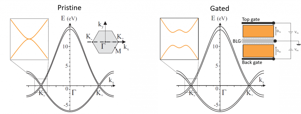
“The problem of edge disorder can be completely circumvented in bilayer graphene”, explains Stampfer, “thanks to the fact that this material is essentially a tunable semiconductor.” In fact, the band-structure of bilayer graphene develops a gap in the presence of a perpendicularly applied electric field (see Figure 3), a feature that allows to use electrostatic gates to create quantum dots, similarly to what is done in silicon and gallium arsenide. In the past decade, several groups have tried this route for creating quantum dots in bilayer graphene. However, until recently essentially all devices were limited by leakage currents due to shortcomings in opening a clean and homogenous gap through the whole device.
What really changed the field were two breakthroughs in year 2013 and 2018. The first one was the development of a dry-stacking methods for sandwiching graphene and other two-dimensional materials between two layers of insulating hexagonal boron nitride (hBN) [4]. This dramatically reduces the detrimental influence of impurities and strain on the properties of the encapsulated material, allowing for devices of extremely high electronic quality. The second one was the idea of using few-layer of graphite placed under the devices as a back gate. This improves substantially the electrostatic coupling to the active layer and, most importantly, it helps screening the residual disorder due to the substrate.
In 2018, the team of Klaus Ensslin at ETH Zürich provided the first clean demonstration of a gate-tunable band-gap in bilayer graphene, realizing the first electrostatically induced quantum point contact [5]. A few months later, the same group reported also the first gate-defined quantum dots in bilayer graphene [6]. “These experiments from the Ensslin group were a real eye opener”, says Stampfer. “They clearly set the direction one needs to go to explore quantum dots – and ultimately qubits – in bilayer graphene”.
The Stampfer group was quick to follow these advancements, publishing its own first results on gate defined quantum dots in bilayer graphene also in 2018 [7]. Since then, the progress has been fast, with more than a dozen papers published by the Ensslin and the Stampfer groups – the two teams that are currently leading the field.
Two of the most recent papers of the Stampfer group have been chosen as Editor’s Pick for the March 2021 edition of Applied Physics Letter [8,9]. “These two works reflect well the current effort in our lab”, says Stampfer, “On one hand we have substantially improved the tunability of our devices, on the other one we are striving to develop advanced sensing techniques to detect the charge state of the dots. The only thing that is still keeping us away from demonstrating a spin qubit in bilayer graphene is fast read out – but we are working on it!“
Confining, manipulating and detecting electrons in bilayer graphene quantum dots
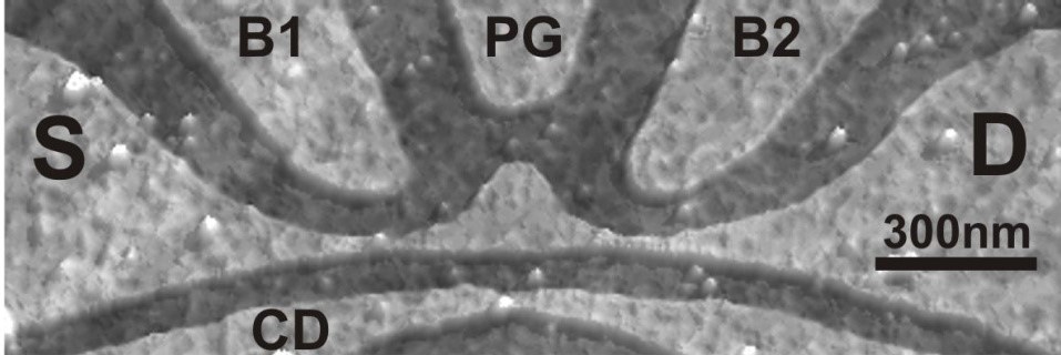
To better understand the advancements of the field, it is worth having a look at how quantum dots in bilayer graphene are formed and investigated. It all starts with a “sandwich” formed by a flake of bilayer graphene between two layers of hexagonal boron nitride (hBN). The sandwich is placed on top of a graphite flake and then holes are drilled into the upper hBN layer, to form Ohmic contacts with the bilayer graphene. A pair of metallic split gates is then deposited on top of the sandwich, separated by a long and narrow constrictions (see Figure 5). These gates are used to introduce a bad gap in the lower laying bilayer graphene, and to form an almost one-dimensional conducting channel between source and drain. Next, one or two layers of metallic finger gates are deposited across the channel, each layer separated by a thin, insulating layer of aluminum oxide (Al2O3). These finger gates are used to modify the energy landscape along the channel, creating narrow regions separated by gapped regions that act as tunneling barriers.
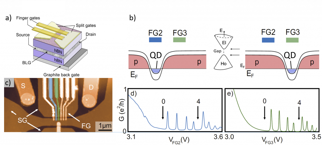
“The initial device design had only one layer of finger gates”, explains Luca Banszerus, who’s leading the bilayer-graphene quantum-dot team in the Stampfer group. “But this limited substantially the possibility of tuning the devices, since we could not tune independently the transparency of the barriers and the potential inside the dot, nor the polarity of the dot itself. That’s why we introduced a second layer of gates, which gives us much more flexibility.”
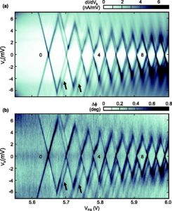
The design of the new devices is illustrated in Figure 6. Their good tunability is one of the results reported in the March issue of Applied Physics Letter [9]. “In this work we focused on the inter-dot coupling between two neighboring quantum dots”, explains Christian Volk, a post-doc in the Stampfer group and lead author of the paper. “Being able to tune this quantity over a wide range is an essential prerequisite for operating a so-called single-triplet qubit, which is one of the most versatile type of spin qubits. With the new design, we obtained a tuning range that is well comparable to what is typical for silicon and GaAs spin qubits.”

The same device allowed also to explore a unique and interesting aspect of bilayer graphene quantum dots, namely the full valley polarization of electrons and holes at moderate magnetic fields [10]. Electron and hole Bloch states in bilayer graphene exhibit, in fact, a topological orbital moment with opposite signs for different valleys as well as for electrons and holes. This causes a large and adjustable effective valley g-factor, which allows to achieve full valley polarization as a function of magnetic field and quasi particle index (electron or holes). This property makes bilayer graphene quantum dots highly interesting for implementing spin-valley qubits – a type of qubit, which should be more resilient to noise than standard spin qubits [11].
“To observe the valley polarization of electrons and holes, it was crucial to be able to tune the quantum dot directly from the few hole regime, through the band gap, into the few electrons regime”, says Banszerus, “which is something we could not achieve with only one layer of finger gates.” Improving the tunability of the devices is only part of the effort of the quantum-dot team in the Stampfer group. To be able to implement spin and spin-valley qubits, it is also necessary to be able to accurately manipulate and detect the state of dots.
For what concerns the manipulation of the dot states, the team has already reached an important milestone demonstrating high-frequency gate manipulation in a single-electron quantum dot in bilayer graphene [12]. This is not only a key requirement for qubit operations, but it also provides information on the excited-states lifetimes in the dot. Applying a megahertz square-pulse to one of the finger gates, Banszerus and co-workers have been able to extract a lower bound for the relaxation time of single-electron spin states in bilayer graphene of 0.5 microseconds.
“This value is very much in line with what extracted from similar experiments in quantum dots in gallium arsenide and in carbon nanotubes”, says Stampfer. “It gives us a lower bound for the spin relaxation time, and tells us that there are no unexpected spin relaxation mechanisms – which is a good, even if unsurprising news. Unfortunately, with the current detection scheme we cannot investigate the true nature of spin relaxation in bilayer graphene. For this, we first need to achieve fast, if not single-shot, readout.”
Single-shot readout means the ability of detecting the occupation of the dot in real time, and is one requirement that is still missing for realizing a spin qubit in bilayer graphene. The reason why it is so important is that, to readout the spin state of an electron in a quantum dot, it is necessary to make a so-called spin-to-charge conversion, whereby the electron is allowed to tunnel in or out of the dot in a way that depends on its spin state. In such a process, detecting the occupation of the dot gives unambiguous information on its spin state – which is one of the DiVincenzo criteria for having a functional spin qubit.
In most of the current experiments, the information on the state of the dot is inferred via transport spectroscopy, i.e. by measuring the current that is flowing through the dot itself. This approach, which requires measuring currents as small as 50 fA, is ultimately limited by the signal-to-noise ratio and can provide information only on the average occupation of the dot. Recently, Banszerus and colleagues have been able to demonstrate a different detection scheme, based on the dispersive read-out of a resonant circuit attached to one of the Ohmic contacts of the dot [8]. This method detects the change in quantum capacitance that occurs when the quantum dot is in resonance with the reservoirs, and an electron can tunnel in or out. The technique turned out to be sensitive enough to accurately resolve the excited-state spectrum of the dot (see Fig. 7), but not for single-shot measurements.
“There is still a lot of room for improvement”, says Banszerus. “It should be possible to gain a lot in sensitivity by improving the resonant circuit, possibly reaching the level needed for single-shot read-out. In parallel, we are going to pursue also the more conventional approach of using a charge detector capacitively coupled to the dot, as it is done in semiconductor qubits. Charge detection in bilayer graphene quantum dot has already been demonstrated by the Ensslin group – even if still with limited bandwidth [13]. I’m pretty confident that, in one way or the other, we are going to reach the single-shot limit.”
This research is to large extent financed by Stampfer’s ERC Consolidator Grant “2D Materials for Quantum Technologies (2D4QT)”. “The goal of 2D4QT is to assess experimentally the potential of graphene-based heterostructures for quantum technology applications”, explains Stampfer. “In other words, we want to give quantitative answers to open questions such as what are the relaxation and coherence times of spin and valley qubits in bilayer graphene, and what can be gained by using isotopically purified carbon. Answering these questions requires continuous technological advancements. The progresses achieved in our lab and at ETH show that we are on the right track. I’m sure that the next years will be full of exciting developments.”
[1] D. P. DiVincenzo, The Physical Implementation of Quantum Computation, Fortschritte der Physik. 48, 771 (2000).
[2] D. Loss and D. P. DiVincenzo, Quantum computation with quantum dots, Phys. Rev. A 57, 120 (1998).
[3] M. Veldhorst et al., A two-qubit logic gate in silicon, Nature 526, 410 (2015); D. M. Zajac et al., Resonantly driven CNOT gate for electron spins, Science 359, 439 (2018); T. F. Watson et al., A programmable two-qubit quantum processor in silicon, Nature 555, 633 (2018).
[4] Wang et al., One-dimensional electrical contact to a two-dimensional material, Science 342, 6158 (2013).
[5] H. Overweg et al., Electrostatically Induced Quantum Point Contacts in Bilayer Graphene, Nano Lett. 18, 553 (2018).
[6] M. Eich et al., Spin and Valley States in Gate-defined Bilayer Graphene Quantum Dots, Phys. Rev. X 8, 031023 (2018).
[7] L. Banszerus et al., Gate-defined electron-hole double dots in bilayer graphene, Nano Lett. 18, 4785 (2018).
[8] L. Banszerus et al., Dispersive sensing of charge states in a bilayer graphene quantum dot, Appl. Phys. Lett. 118, 093104 (2021).
[9] L. Banszerus et al., Tunable interdot coupling in few-electron bilayer graphene double quantum dots, Appl. Phys. Lett. 118, 103101 (2021).
[10] L. Banszerus et al., Electron-hole crossover in gate-controlled bilayer graphene quantum dots, Nano Lett. 10, 7709 (2020).
[11] D. Culcer et al, Valley-Based Noise-Resistant Quantum Computation Using Si Quantum Dots, Phys. Rev. Lett. 108, 126804 (2012); N. Rohling, and G. Burkard, Universal quantum computing with spin and valley states, New J. Phys. 14, 083008 (2012).
[12] L. Banszerus et al., Pulsed-gate spectroscopy of single-electron spin states in bilayer graphene quantum dots, Phys. Rev. B 103, L081404 (2021).
[13] A. Kurzmann et al. , Charge Detection in Gate-Defined Bilayer Graphene Quantum Dots, Nano Lett. 19, 5216 (2019).