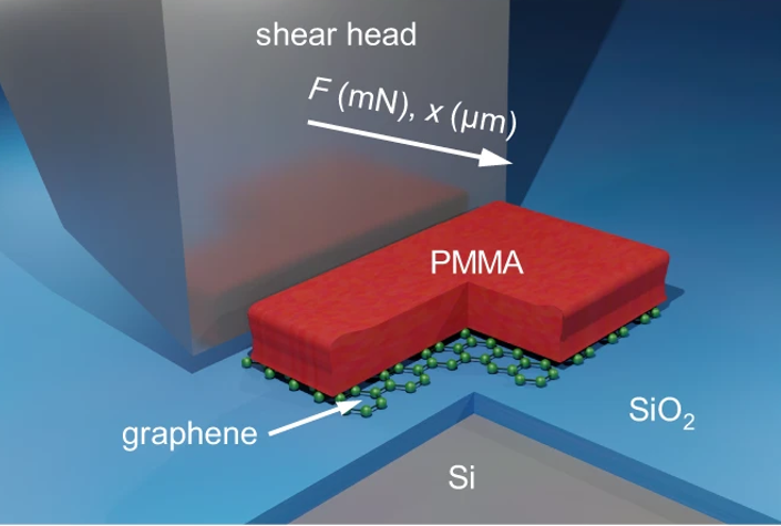
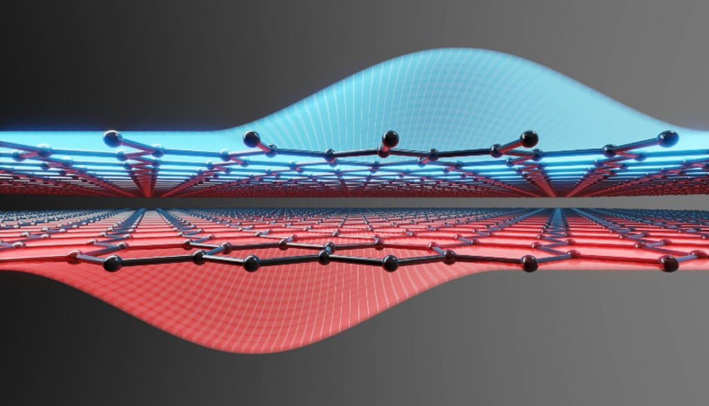
A scalable pathway for the mechanical transfer of graphene grown by CVD 

Nowadays it is possible to grow high-quality graphene on large scale using chemical vapor deposition (CVD). What remains a major bottleneck for the industrialization of the material is the transfer of graphene from the growth substrate to a target one. A team of researchers from the University of Cambridge and RWTH Aachen University has now developed a methodology for optimizing simultaneously the growth and the transfer process, showing that it is possible to dry-transfer graphene with high-yield, if the crystallographic orientation of the growth surface is chosen appropriately.

Optical micrograph of star-shaped graphene flakes grown by CVD on copper.
(© Stampfer Lab, RWTH Aachen University) 
Continue reading “A scalable pathway for the mechanical transfer of graphene grown by CVD “

First experimental observation of an elusive stacking order in tetralayer graphene

Using advanced spectroscopic techniques, researchers from RWTH Aachen University have been able to observe for the first-time domains of tetralayer graphene with ABCB stacking. The results have been reported in ACS Nano.

s-SNOM imaging of different stacking domains in tetralayer graphene. The highlighted domain and schematics on the right correspond to ABCB stacking .
Continue reading “First experimental observation of an elusive stacking order in tetralayer graphene”

How to report and benchmark emerging field-effect transistors

One of the challenges encountered by research on novel electronic devices is to compare devices based on different materials in a consistent way. RWTH Professor Max Lemme and colleagues from USA, China, and Belgium have now proposed a set of clear guidelines for benchmarking key parameters and performance metrics of emergent field-effect transistors. The guidelines have been published as a Perspective Article in Nature Electronics.

Continue reading “How to report and benchmark emerging field-effect transistors”

New perspectives on Layer Transfer and Artificial Crystalline Heterostructures at IKZ – A talk by Dr. Jens Martin

Dr. Jens Martin, from the Leibniz-Insitut für Kristallforschung (IKZ) in Berlin, has been the speaker of the 30th Aachen Graphene Center Seminar. Dr. Martin is the head of the section Semiconductor Nanostructures at IKZ, and one of the coordinators of the IKZ-IRIS Joint Lab “Layer Transfer for 2D-Heterostructures“.  In his talk, presented the recent advances of his group on the growth, release and transfer of thin epitaxial perovskite films, as well in on the in-situ growth of 2D-vdW multilayers and heterostructures.

Continue reading “New perspectives on Layer Transfer and Artificial Crystalline Heterostructures at IKZ – A talk by Dr. Jens Martin”

A major event on graphene in Aachen

AMO GmbH is one of the organizer of Graphene 2022, Europe’s largest conference on graphene and 2D materials, which is taking place in Aachen from July 5 to 8, 2022. More than 500 scientist have gathered at the Eurogress for four intensive days of scientific discussions. The conference program features 76 speakers – including the 2010 Nobel Prize laureate in physics, Professor Andre Geim, and Professor Pablo Jarillo-Herrero from MIT – as well as six workshops, an industrial forum and 33 exhibitors from across the globe.  

Continue reading “A major event on graphene in Aachen”